NCP1603
http://onsemi.com
24
Feedback in PFC Section
The output voltage of the PFC circuit (i.e., bulk voltage
V
bulk
) is sensed as a feedback current I
FB1
flowing into the
FB1 pin (Pin 9) of NCP1603. The FB1 pin voltage V
FB1
is
typically smaller than 5.0 V referring to Figure 31. It is
much lower than V
bulk
that is typically 400 V. Therefore,
V
FB1
is generally neglected.
I
FB1
+
V
bulk
* V
FB1
R
FB1
[
V
bulk
R
FB1
(eq. 19)
where R
FB1
is the feedback resistor connected the FB1 pin
(Pin 9) and the output voltage referring to Figure 45.
Then, the feedback current I
FB1
represents the bulk
voltage V
bulk
and will be used in the PFC section voltage
regulation, undervoltage protection (UVP), and
overvoltage protection (OVP).
Bulk Voltage Regulation in PFC Section
PFCstage feedback current I
FB1
, that presents bulk
voltage V
bulk
or the PFCstage output voltage, is regulated
with a reference current (I
ref
= 203 mA typical) as shown in
Figure 63. When I
FB1
is lower than 96% of I
ref
, the V
reg
that
is the output of the regulation block is as high as
V
control(max)
(1.05 V typical) that it gives the maximum
value on V
ton
and the maximum MOSFET on time and
V
bulk
increases. When I
FB1
is higher than I
ref
, the V
reg
becomes 0 V that gives no MOSFET on time and V
bulk
decreases. As a result, the bulk voltage V
bulk
is regulated
around the range between 96% and 100% of the nominal
value of R
FB1
?/SPAN> I
ref
.
Figure 63. Regulation Block
V
reg
I
ref
I
ref
96%
I
FB1
1 V
Based on Equations 13 and 14 for a particular power
level, the V
control
is inversely proportional to V
ac
2
. Hence,
in high V
ac
condition V
control
is lower. It means that I
FB1
or
output voltage is higher based on the regulation block
characteristic in Figure 63. In other words, the V
control
in
the low V
ac
condition is much higher than the high V
ac
condition. In order to not overdesign the circuit in the
application, the V
control
in the low V
ac
condition is usually
very closed to V
control(max)
. It makes the output voltage be
almost 96% of the nominal value of R
FB1
?I
ref
in high V
ac
condition.
The feedback resistor R
FB1
consists of two or three high
precision resistors in order to set the nominal V
bulk
precisely and for safety purpose.
The regulation block output V
reg
is connected to control
voltage V
control
through an internal resistor R
control
(300 kW typical) for the lowpass filter in Figure 62. The
V
control
and the time information of zero current are
collected in the V
control
processing circuit to generate V
ton
that is then compared to a ramp signal to generate the
MOSFET on time t
1
for power factor correction.
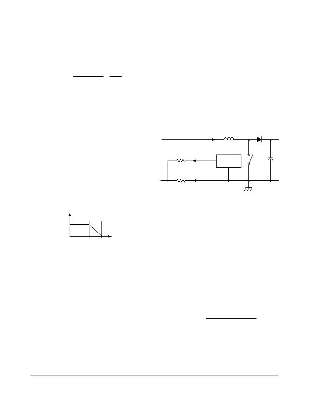
Current Sense in PFC Section
The PFC section senses the inductor current I
L
by the
current sense scheme in Figure 64. This scheme has the
advantages of: (1) the inrush current limitation by the
resistor. R
CS1
. and (2) the overcurrent protection and zero
current detection implemented in the same pin.
Figure 64. Current Sense in PFC Section
CS1
NCP1603
Gnd1
+
R
CS1
R
S1
I
L
I
S
I
L
V
S
Inductor current I
L
passes through R
CS1
and creates a
negative voltage. This voltage is measured by a current I
S
flowing out of the CS1 pin (Pin 11). CS1 pin has an offset
voltage V
S
. This offset voltage is studied in the setting of
zero inductor current I
L(ZCD)
and the maximum inductor
current I
L(OCP)
(i.e., overcurrent protection threshold). A
typical variation of offset voltage V
S
versus sense current
I
S
is shown in Figure 35. Based on Figure 64, Equation 20
is derived.
V
S
* R
S1
I
S
+ R
CS1
I
L
(eq. 20)
Zero Current Detection (ZCD) in PFC Section
The device recognizes zero inductor current when CS1
pin (Pin 11) sense current I
S
is smaller than I
S(ZCD)
(14 mA
typical). The offset voltage of the CS1 pin in this condition
is V
S(ZCD)
(7.5 mV typical). The inductor current I
L(ZCD)
at the ZCD condition is derived in Equation 21.
I
L(ZCD)
+
R
S1
I
S(ZCD)
* V
S(ZCD)
R
CS1
(eq. 21)
发布紧急采购,3分钟左右您将得到回复。
相关PDF资料
NCP1605DR2G
IC PFC CONTROLLER CCM/DCM 16SOIC
NCP1606BDR2G
IC POWER FACTOR CONTROLLER 8SOIC
NCP1607BDR2G
IC PFC CONTROLLER CRM 8SOIC
NCP1611BDR2G
IC PFC CTLR HE ENHANCED 8-SOIC
NCP1651DR2G
IC PFC CONTROLLER CCM/DCM 16SOIC
NCP1654BD133R2G
IC PFC CCM 133KHZ 8-SOIC
NCP1927DR2G
IC CTLR PFC/FLYBACK 16-SOIC
NCP380HMU21AATBG
IC CURRENT LIMIT SWITCH 6-UDFN
相关代理商/技术参数
NCP1605ADR2G
功能描述:功率因数校正 IC ENHANCED PFC CNTRLER RoHS:否 制造商:Fairchild Semiconductor 开关频率:300 KHz 最大功率耗散: 最大工作温度:+ 125 C 安装风格:SMD/SMT 封装 / 箱体:SOIC-8 封装:Reel
NCP1605BDR2G
功能描述:功率因数校正 IC High Volt Stby Mode Power Fact Corr Cont RoHS:否 制造商:Fairchild Semiconductor 开关频率:300 KHz 最大功率耗散: 最大工作温度:+ 125 C 安装风格:SMD/SMT 封装 / 箱体:SOIC-8 封装:Reel
NCP1605DR2G
功能描述:功率因数校正 IC Enhanced PFC HV and Eff Standby RoHS:否 制造商:Fairchild Semiconductor 开关频率:300 KHz 最大功率耗散: 最大工作温度:+ 125 C 安装风格:SMD/SMT 封装 / 箱体:SOIC-8 封装:Reel
NCP1605FORWGEVB
功能描述:电源管理IC开发工具 NCP1605 152 W FORWARD EVB
RoHS:否 制造商:Maxim Integrated 产品:Evaluation Kits 类型:Battery Management 工具用于评估:MAX17710GB 输入电压: 输出电压:1.8 V
NCP1605LCDTVGEVB
功能描述:BOARD EVAL NCP1605/1396 RoHS:是 类别:编程器,开发系统 >> 评估演示板和套件 系列:* 产品培训模块:Obsolescence Mitigation Program 标准包装:1 系列:- 主要目的:电源管理,电池充电器 嵌入式:否 已用 IC / 零件:MAX8903A 主要属性:1 芯锂离子电池 次要属性:状态 LED 已供物品:板
NCP1606ADR2G
功能描述:功率因数校正 IC PWR FCTR CONTROLLER RoHS:否 制造商:Fairchild Semiconductor 开关频率:300 KHz 最大功率耗散: 最大工作温度:+ 125 C 安装风格:SMD/SMT 封装 / 箱体:SOIC-8 封装:Reel
NCP1606APG
功能描述:功率因数校正 IC LO CST PWR FCTR CONT RoHS:否 制造商:Fairchild Semiconductor 开关频率:300 KHz 最大功率耗散: 最大工作温度:+ 125 C 安装风格:SMD/SMT 封装 / 箱体:SOIC-8 封装:Reel
NCP1606BDR2G
功能描述:功率因数校正 IC PWR FCTR CONTROLLER RoHS:否 制造商:Fairchild Semiconductor 开关频率:300 KHz 最大功率耗散: 最大工作温度:+ 125 C 安装风格:SMD/SMT 封装 / 箱体:SOIC-8 封装:Reel